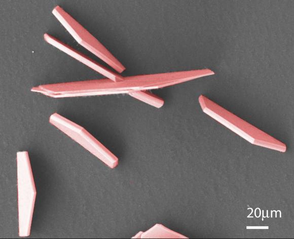
PROVIDENCE, R.I. [Brown University] — Chemists from Brown University have found a way to make new 2-D, graphene-like semiconducting nanomaterials using an old standby of the semiconductor world: silicon.
In a paper published in the journal Nanoletters, the researchers describe methods for making nanoribbons and nanoplates from a compound called silicon telluride. The materials are pure, p-type semiconductors (positive charge carriers) that could be used in a variety of electronic and optical devices. Their layered structure can take up lithium and magnesium, meaning it could also be used to make electrodes in those types of batteries.
“Silicon-based compounds are the backbone of modern electronics processing,” said Kristie Koski, assistant professor of chemistry at Brown, who led the work. “Silicon telluride is in that family of compounds, and we’ve shown a totally new method for using it to make layered, two-dimensional nanomaterials.”
Koski and her team synthesized the new materials through vapor deposition in a tube furnace. When heated in the tube, silicon and tellurium vaporize and react to make a precursor compound that is deposited on a substrate by an argon carrier gas. The silicon telluride then grows from the precursor compound.
Different structures can be made by varying the furnace temperature and using different treatments of the substrate. By tweaking the process, the researchers made nanoribbons that are about 50 to 1,000 nanometers in width and about 10 microns long. They also made nanoplates flat on the substrate and standing upright.
“We see the standing plates a lot,” Koski said. “They’re half hexagons sitting upright on the substrate. They look a little like a graveyard.”
Each of the different shapes has a different orientation of the material’s crystalline structure. As a result, they all have different properties and could be used in different applications.
The researchers also showed that the material can be “doped” through the use of different substrates. Doping is a process through which tiny impurities are introduced to change a material’s electrical properties. In this case, the researchers showed that silicon telluride can be doped with aluminum when grown on a sapphire substrate. That process could be used, for example, to change the material from a p-type semiconductor (one with positive charge carriers) to an n-type (one with negative charge carriers).
The materials are not particularly stable out in the environment, Koski says, but that’s easily remedied.
“What we can do is oxidize the silicon telluride and then bake off the tellurium, leaving a coating of silicon oxide,” she said. “That coating protects it and it stays pretty stable.”
From here, Koski and her team plan to continue testing the material’s electronic and optical properties. They’re encouraged by what they’ve seen so far.
“We think this is a good candidate for bringing the properties of 2-D materials into the realm of electronics,” Koski said.
Koski’s co-authors on the paper were postdoctoral researcher Sean Keuleyan, graduate student Mengjing Wang, and undergraduates Frank Chung and Jeffrey Commons.

