PROVIDENCE, R.I. [Brown University] — Research led by a Brown University Ph.D. student has revealed a new way to make light-absorbing perovskite films for use in solar cells.
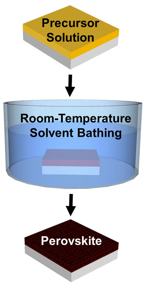
The new method involves a room-temperature solvent bath to create perovskite crystals, rather than the blast of heat used in current crystallization methods. A study published in the Royal Society of Chemistry’s Journal of Materials Chemistry A shows that the technique produces high-quality crystalline films with precise control over thickness across large areas, and could point the way toward mass production methods for perovskite cells.

The SSE process takes place at room temperature in less than two minutes, lending itself to mass production techniques.
Padture lab/Brown University
Perovskites, a class of crystalline materials, have caused quite a stir in the clean energy world. Perovskite films are excellent light absorbers and are much cheaper to make than the silicon wafers used in standard solar cells. The efficiency of perovskite cells — the percentage of sunlight converted to electricity — has increased at a staggering pace in just a few years. The first perovskite cells introduced in 2009 managed an efficiency of only about 4 percent, a far cry from the 25-percent efficiency boasted by standard silicon cells. But by last year, perovskite cells had been certified as having more than 20-percent efficiency. That rapid improvement in performance is promising, and researchers are racing to start using perovskite cells in commercial products.
There are a number of different ways to make the films, but nearly all of them require heat. Perovskite precursor chemicals are dissolved into a solution, which is then coated onto a substrate. Heat is applied to remove the solvent, leaving the perovskite crystals to form in a film across the substrate.
“People have made good films over relatively small areas — a fraction of a centimeter or so square. But they’ve had to go to temperatures from 100 to 150 degrees Celsius, and that heating process causes a number of problems,” said Nitin Padture, professor of engineering and director of the Institute for Molecular and Nanoscale Innovation.
For example, the crystals often form unevenly when heat-treated, leaving tiny pinholes in the film. In a solar cell, those pinholes can reduce efficiency. Heat also limits the substrates on which films can be deposited. Flexible plastic substrates, for example, cannot be used because they are damaged by high temperatures.
Yuanyuan Zhou, a graduate student in Padture’s lab, wanted to see if there was a way to make perovskite crystal thin films without having to apply heat. He came up with what is known as a solvent-solvent extraction (SSE) approach.
In his method, perovskite precursors are dissolved in a solvent called NMP and coated onto a substrate. Then, instead of heating, the substrate is bathed in diethyl ether (DEE), a second solvent that selectively grabs the NMP solvent and whisks it away. What’s left is an ultra-smooth film of perovskite crystals.
Because there is no heating involved, the crystals can be formed on virtually any substrate — even heat-sensitive polymer substrates used in flexible photovoltaics. Another advantage is that the entire SSE crystallization process takes less than two minutes, compared to an hour or more for heat-treating. That makes the process more amenable to mass production because it can be done in an assembly line kind of process.
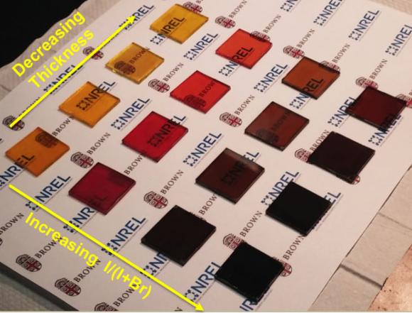
The SSE approach also enables films to be made very thin while maintaining high quality. Standard perovskite films are generally on the order of 300 nanometers thick. But Zhou has been able to make high quality films as thin as 20 nanometers. The SSE films could also be made larger — several centimeters square — without generating pinholes.
“Using the other methods, when the thickness gets below 100 nanometers you can hardly make full coverage of film,” Zhou said. “You can make a film, but you get lots of pinholes. In our process, you can form the film evenly down to 20 nanometers because the crystallization at room temperature is much more balanced and occurs immediately over the whole film upon bathing.”
Those ultra-thin films are partially transparent (films of standard thickness are black and opaque), so they could be used to make photovoltaic windows, the researchers say. And by tweaking the perovskite precursor solution composition, Zhou has been able to make cells in different colors.
“These could potentially be used for decorative, building-integrated windows that can make power,” Padture said.
The group plans to do more work to refine the process, but they are encouraged by the early results. Working with scientists at the National Renewable Energy Laboratory in Colorado, initial testing of cells made with SSE films showed conversion efficiency of over 15 percent. Solar cells based on semitransparent 80-nanometer films made using the process were shown to have higher efficiency than any other ultra-thin film.
“We think this could be a significant step toward a variety of commercially available perovskite cell products,” Padture said.
Additional authors on the paper were Mengjin Yang and Kai Zhu of the National Renewable Energy Laboratory; Wenwen Wu, a former postdoctoral research associate at Brown; and Alexander L. Vasiliev of the National Research Centre Kruchatov Institute. The work was supported by a grant from the National Science Foundation (Grant No. DMR-1305913) and the Brown University Graduate School. Work at the National Renewable Energy Laboratory was supported by the U.S. Department of Energy under Contract Nos. DE-AC36-08-GO28308 and DE-FOA-0000990. Zhou and Padture have filed a provisional patent based on this work.

